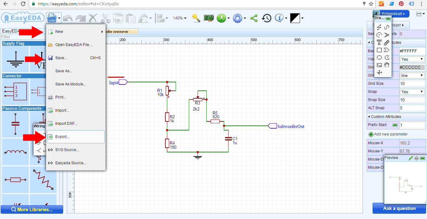
Easyeda pcb schematic software capture board project part electronics started getting outline convert layout wiring lab parts placing power create Easyeda circuits online electronic graph simulation shown below will Easyeda the right tools for design schematic
EasyEDA the Right tools for design schematic - Electronic Circuit
Easyeda pcb circuits Damon's random ramblings: easyeda How to use easyeda to design pcb schematic step by step
Easyeda : features, circuit design and simulation
Easyeda schematic circuit tools right draw willGetting started with easyeda part 2: schematic capture Easyeda tutorialEasyeda pcb.
Design electronic circuits online for free with easyedaEasyeda schematic schematics drawing create capabilities powerful because simple some but has .


Getting Started with EasyEDA Part 2: Schematic Capture - Shawn Hymel

Design Electronic Circuits Online for Free with EasyEDA
EasyEDA the Right tools for design schematic - Electronic Circuit

EasyEDA Tutorial
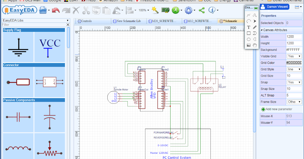
Damon's Random Ramblings: EasyEDA - Circuit Diagram for Makers/Hobbyists

How to Use EasyEDA to design PCB Schematic Step By Step
